





Pinned Tweet
🚀 EasyEDA Spark 2026 is LIVE!
🏆 Compete for a share of the $85,000 prize pool
📦 Material & shipping support
🎁 $100 JLCPCB coupon for every completed project
🏭 JLCPCB Factory Tour
🌍 EasyEDA Spark Conference 2027
🔗 oshwlab.com/activities/easye…
#EasyEDASpark #JLCPCB #OSHWLab

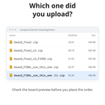
Naming Gerber files: a skill nobody teaches. 📁
Which one did you actually upload? 👀
Our quote page previews whatever you upload. That's the moment to find out which "final" it was, not when the boards arrive.
#EngineeringHumor #JLCPCB

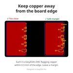
Keep parts and traces away from the board edge. 📏
Routing the outline can damage anything that sits too close.
For JLCPCB orders, keep copper at least 0.2 mm from routed edges and 0.4 mm from V-cut edges. More is safer.
#PCBDesign #DFM #JLCPCB


Controlled Impedance Is More Than Trace Width!
Stackup, dielectric, copper thickness, and reference planes all affect impedance.
Keep planes continuous and design for your target impedance.
#PCBDesign #HighSpeedDesign #JLCPCB

What is Via-in-Pad? 👀
A via placed directly inside a component pad can help save PCB space and simplify routing in compact designs.
Want to learn more about this PCB design technique? Save this video for later! 📌
Read more about via-in-pad:
jlcpcb.com/help/article/via-…
#JLCPCB
Tried adding resistors to connect I2C & UART. We tried to talk, but we still can’t understand each other. We’re done. You don’t get me at all.
Just for fun, resistors won’t save this 😂
#ElectronicsMeme #JLCPCB

How does a thin PI heater generate heat? 🔍
A patterned metal trace converts electrical energy into heat as current flows. PI films provide insulation, while lead wires connect the heater to a power source.
Learn more 👇
jlcpcb.com/blog/what-are-fle…
#Engineering #FlexibleHeater

LDO capacitors do more than filter noise. ⚡
They also help with load transient response and loop stability.
But bigger isn't always better — the right capacitance and ESR depend on the LDO datasheet.
Don't overlook those caps!
#JLCPCB #PCBDesign #electronics

When your I2C slave sends an ACK.
111011...
111111...
Continue, I'm listening.😏
Who’s debugged I2C at 2 AM?
Drop a comment!
#Electronics #Embedded #I2C #HardwareMeme #JLCPCB

A 10 Euro cent for scale. 📏
01005 components. 0.5mm FPC. 3x3 BGA.
Our SMT machines place them all with absolute precision. 🤖
What's the smallest package you've hand-soldered? 👇
#PCBDesign #SMT #JLCPCB

ALT The image shows a white JLPCB circuit board featuring two FPC connectors, labeled with various component specifications including "01005," "0402," "0603," "RF coupler," "TVS/ESD," and "Balun." A 10 Euro cent coin is placed beside it for scale.
Your 4-layer board went through a press like this. 🔥
Inner core + prepreg (resin-soaked glass fabric) + copper foils, under controlled heat and pressure.
The resin fills the gaps, cures, and fuses it all into one board.
#MultilayerPCB #JLCPCB


SPOT THE DRC BLIND SPOT! 🔍☕🤯Look closely at the PA8 trace & via. Which layout is flawed: A or B? 👇(Answer pinned in 24 hrs!)#PCBDesign #JLCPCB #Electronics #EE #SpotTheDifference #EasyEDA

Avoid sharp acute angles in your traces. 📐
They can trap etchant in fabrication (acid traps). Use 45° turns or smooth curves.
Before you order, our free JLCDFM check reviews your traces, drilling, solder mask and silkscreen.
#PCBDesign #JLCPCB


Roses are red, violets are blue… 🌹
We make PCBs. So here's a bouquet for you! 💐
#JLCPCB #PCB #Electronics

ALT A bouquet of purple and white flowers mixed with various colorful printed circuit boards, displayed on a dark surface. The JLCPCB logo is visible in the top left corner.

ALT A unique bouquet arrangement featuring a mix of pastel flowers interspersed with colorful computer circuit boards. The bouquet is displayed on a table with technical drawings and additional circuit boards in the background.