







Pinned Tweet
I excited to work with @SEMIconex team and Technical Community on our latest semiconductor challenges and solutions!

We are pleased to welcome Beth Keser as VP, Technology Coalitions.
Beth is a recognized global semiconductor leader with more than 30 years of experience in advanced packaging, chiplets, and heterogeneous integration. An IEEE Fellow and accomplished industry executive, Beth has held senior technology leadership roles at Motorola, Qualcomm, and Intel, holds more than 50 U.S. patents and patents pending, and has been widely recognized for her contributions to advancing semiconductor packaging technologies.
In this role, Beth will continue to strengthen SEMI’s ability to bring members and industry stakeholders together around the technology challenges and opportunities shaping the future of the semiconductor ecosystem. She will lead SEMI’s Technology Coalitions, Smart Initiatives, Standards, strategic collaborations and public-private R&D partnerships, building on the work already underway to accelerate collective solutions, expand industry participation, and advance SEMI’s thought leadership as the industry evolves. Beth has already jumped into her role meeting with members at recent SEMI events.
Beth remarked: “I’m excited to join SEMI at such an important time for our industry. After decades focused on advancing semiconductor technology from the back end, I’m looking forward to bringing that perspective to a broader ecosystem—connecting technology, industry leaders, and end markets to help address the challenges and opportunities ahead.”
Please join us in welcoming Beth to SEMI.


Looking to collab on a semi RnD idea? Call Fraunhofer IPMS or IZM! ipms.fraunhofer.de/en/press-…
Element 6 (think diamond) and Entegris Announce Strategic Collab (think GPU cooling) e6.com/en/about/news/element…

Marvell in talks to buy Lumentum for $80B stocks.apple.com/A_V_-jR-PQ-…


Foundries And OSATs Increasingly Overlap semiengineering.com/foundrie…

Beth Keser retweeted

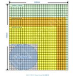
ASE showcased its panel-level packaging (PLP) solution for AMD’s Venice CPU, with initial production targeted for Q1 2027, likely at limited scale at its Kaohsiung facility. ASE and its subsidiary SPIL have worked with AMD to implement the second generation of their Fan-Out Embedded Bridge (FOEB) technology in Venice. The current 310 × 310 mm panel accommodates 25 Venice interposers after edge loss, compared with 22 on a traditional round 300 mm carrier wafer, roughly a 14% increase in gross package count. This modest improvement in package output per carrier represents a starting point for panel-level interposers with Venice’s 2.7x reticle size, rather than evidence of a dramatic reduction in cost. (1/2)🧵
Source: OCP ASE Booth

What Breaks When Packaging Moves From Wafer To Panel? semiengineering.com/what-bre…

Increase in TSMC advanced packaging pricing expected. finance.yahoo.com/technology…

The imec Report: Scaling Optical Interconnects For The AI Era semiengineering.com/the-imec…

Data Center Power a Prominent Highlight of OCP 2026 eetimes.com/data-center-powe…

Beth Keser retweeted

SEMICON West 2026, right at your fingertips.
🔗 semiconwest.org/about/mobile…
Download the mobile app to build your agenda, explore exhibitors, navigate the show floor, and connect with attendees. Already have it? Select the 2026 event and enable notifications for show updates.
Follow @SEMIAmericas and use the official show hashtag #SEMICONWest to join the conversation.
We'll be seeing you in San Francisco!

Go through security without a boarding pass? So retro! tsa.gov/precheck/gateside-ts…

SEMI launches chip materials alliance taipeitimes.com/News/biz/arc…

“The old rule that scale-up is copper and scale-out is optical is starting to blur. As data rates climb inside the rack, copper is running into physical limits around loss, reach, and power, challenging the ability of copper within a rack." semiengineering.com/coppers-…


Beth Keser retweeted

NVIDIA Spectrum-X Ethernet Photonics is now in full production.
4x fewer lasers. 5x lower power. 10x higher mean time between incidents.
See how we built it ▶️ nvda.ws/45so1a7

