

Join us as we reforge the semiconductor story, from ideas to chips
Mahape, Navi Mumbai
Joined March 2024
- Tweets449
- Following4
- Followers487
- Likes179




Semiconductor Molding: Protecting Semiconductor Devices
Molding is an important process in semiconductor packaging that encapsulates the fabricated die and its interconnections within a protective material.

1
44
Big celebrations? Not always needed. A little appreciation goes a long way! 💙
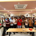
At @rrpelectronic , we celebrated International Men's Day in our own simple yet special way, appreciating the men who support, inspire and make a difference every day.
Happy International Men's Day

69
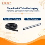
Tape & Reel Packaging involves placing components into individual pockets of a carrier tape, securing them with a cover tape and winding the tape onto a reel.
Tube Packaging involves arranging semiconductor components within protective tubes.

54
RRP Electronics offers Flip-Chip Bonding, which connects fabricated dies to substrates using conductive bumps, and Wire Bonding, which uses fine wires to create electrical pathways in packaged semiconductor components and modules for system-level integration.

1
89
Epoxy Bonding
Epoxy bonding uses specialised adhesive materials to attach or secure components within a semiconductor package, depending on the package design and assembly requirements.

1
102
Honouring the special bond that grows stronger with every moment, every smile and every celebration.
May the bond between siblings always shine bright.
Happy Bhai Dooj!
#HappyBhaiDooj #BhaiDooj #SiblingBond #FestivalOfLove #CelebrationOfTogetherness #FestiveWishes

126
Stack Bonding is an advanced semiconductor packaging process that involves vertically integrating multiple semiconductor dies within a single package.
By combining dies in a stacked configuration, this approach enables higher component integration and compact package designs.

1
101
The RRP team came together to celebrate Diwali with a traditional pooja ceremony, seeking blessings. The celebrations continued with interactive games and fun-filled festive activities, making the occasion memorable through shared laughter and team bonding.

1
102
May the divine blessings of Goddess Lakshmi bring prosperity, happiness and abundance into every home.
May the light of Diwali illuminate new opportunities and inspire success in every endeavour.
Wishing you and your family a very Happy Diwali and Shubh Laxmi Poojan! 🪔✨

75
A celebration of prosperity, a symbol of good fortune and a beginning of new possibilities.
Wishing everyone a joyful and prosperous Dhanteras!
#Dhanteras #FestiveGreetings #NewBeginnings #semiconductors #Prosperity #RRPElectronics

1
120
Wafer Grinding: Preparing Semiconductor Wafers for Packaging
Wafer grinding is a controlled material-removal process used to reduce the thickness of a fabricated semiconductor wafer according to specific requirements.

109
Ball Grid Array technology uses an array of solder balls on the underside of a semiconductor package to establish electrical and mechanical connections with a printed circuit board.
An advanced variation, Flip-Chip BGA, combines flip-chip die interconnection with a BGA package.

133
Understanding LGA Packaging
Land Grid Array (LGA) packaging uses an array of flat electrical contact pads on the underside of the package to establish connections with a compatible PCB or socket.

130
QFN vs DFN PACKAGING
Compact Design. Precise Interconnections.
QFN — Quad Flat No-Lead
Contact lands typically arranged along four sides.
DFN — Dual Flat No-Lead
Contact lands typically arranged along two opposing sides.

1
143
SIM vs eSIM
Traditional removable SIM cards are available in different physical formats. These cards are inserted into compatible devices.
Embedded SIM technology takes a different approach by integrating the SIM module into the device.

114
Embedded SIM technology is transforming how devices connect, enabling compact designs and seamless integration across connected applications.

2
146
WIRE-BONDED SIM MODULES | Proven Technology. Scalable Manufacturing.
Wire bonding remains an established semiconductor packaging technology, enabling reliable electrical interconnections for SIM module assembly.

2
143
FLIP-CHIP BONDED SIM MODULES
Flip-chip bonding enables direct die-to-substrate interconnection, supporting compact module designs and shorter electrical interconnects.

143
NAVRATRI CELEBRATIONS
Beginning with prayers and blessings, and continuing with the rhythm of Garba!
A beautiful celebration of culture, positivity, and togetherness at RRP Electronics.
137
